| Year | Authors | Title | IGZO | |||||||||||||||||||
| 2016 TIT, Japan
|
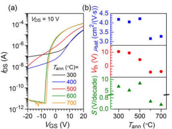
Haochun Tang, Keisuke Ide, Hidenori Hiramatsu a,b, Shigenori Ueda, Naoki Ohashi, Hideya Kumomi, Hideo Hosono, Toshio Kamiya | Effects ofthermal annealing on elimination ofdeep defects in amorphous In–Ga–Zn–Othin-film transistors |
IGZO condition
|
 |
||||||||||||||||||
| 2015 Fudan U. Shanghai
|
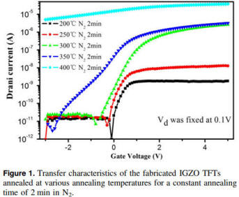
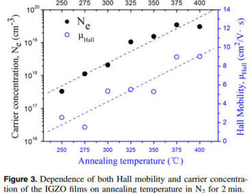
Wen-Peng Zhang, Sun Chen, Shi-Bing Qian and Shi-Jin Ding | Effects of thermal annealing on the electrical characteristics of In-Ga-Zn-O thin-film transistors with Al2O3 gate dielectric |
IGZO condition
|
 |
||||||||||||||||||
| 2012 Taiwan
|
Chien-Hung Wua, Kow-Ming Chang, Sung-Hung Huangb,
I-Chung Deng, Chin-Jyi Wue, Wei-Han Chiang, Je-Wei Line and Chia-Chiang Change |
The effect of thermal annealing on the properties of IGZO TFT
prepared by atmospheric pressure plasma jet |
IGZO condition
|
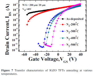
 The threshold voltage (VT) shifting more positive after post annealing means that free electron carriers are reduced. The free carriers maybe result from oxygen vacancy or H-related species, and the carrier concentration was reduced effectively by post annealing. As a result, the switching behavior was improved. |
||||||||||||||||||